Time: : 2:00-4:00pm,march29th,2012(Thursday)
Place:748 Room, ICT, CAS
Speaker:Xiaoqing Wen
Abstract:
Low-powerVLSIcircuitsareindispensablefor modern electronic devices, and numeroushardware/software-based techniques have been developed for drastically reducing functional power dissipation. However, testing such low-power devices has increasingly become a severe challenge, especially in at-speed scan testing where a transition is launched at the output of a flip-flop and the corresponding circuit response is captured by a flip-flop with a functional clock pulse. The reason is that functional constraints with respect to circuit operations and clocking are mostly ignored in at-speed scan testing, which may result in test power that is 3X to 8X higher than functional power. Excessive test power may cause die/package damage due to excessive heat as well as undue yield loss due to excessive power supply noise, as illustrated in Figure 1. This clearly indicates that low-power VLSI designs cannot be successfully realized without effective and efficient low-power testing.
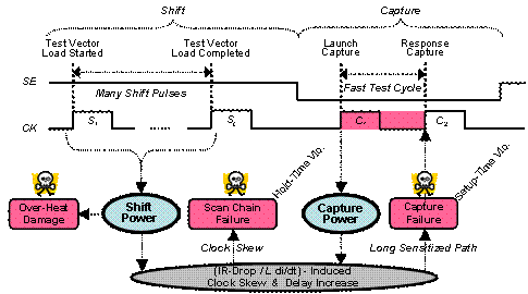
Figure 1. Impact of Test Power in Launch-on-Capture-Based At-Speed Scan Testing
This presentation first describes the basics of power dissipation in CMOS VLSI circuits. It goes on to highlight the difference between power dissipation in function mode and power dissipation in test mode, and lists the reasons why test power often become much higher than functional power for low-power VLSI circuits. This presentation then describes the widely used clocking scheme for at-speed scan testing, namely launch-on-capture (LOC), and shows the different characteristics of shift power and capture power in LOC-based at-speed scan testing. Based on that, a general low-power testing strategy is outlined, featuring the use of design-for-test (DFT) for reducing shift power and the use of test data manipulation for reducing capture power. This presentation then shows a few examples of state-of-the-art low-power test techniques for reducing shift and capture power. Finally, this presentation discusses future trends in the research and development of more advanced and sophisticated low-power test solutions for future low-power VLSI circuits.
bio:
Xiaoqing Wen received his B.E. degree from Tsinghua University, China, in 1986, his M.E degree from Hiroshima University, Japan, in 1990, and his Ph.D. degree from Osaka University, Japan, in 1993. He is currently a Professor at Kyushu Institute of Technology (KIT), Japan. Prior to joining KIT, he was with SynTest Technologies, Inc. (Sunnyvale, USA) for six years and served as Chief Technology Officer until 2003. Prof. Wen holds 31 US patents and 3 Japan patents on VLSI testing, most of them being used in commercial VLSI test design tools and 6 of them being licensed to LPTEX. He received the 2008 IEICE Information & Systems Society Best Paper Award for his research in low-power testing. He co-edited/co-authored two books: one on general VLSI testing and one on low-power testing. He is a Fellow of IEEE.